PCB Layer Stackup
Design a layer stackup to your impedance targets from manufacturer laminate data.
What it's for
Design a PCB layer stackup to your impedance targets from manufacturer laminate data. Set the layer count (or let it be recommended from BGA escape), finished thickness, copper weights, and core and prepreg materials, then add impedance targets — typed in, imported from the node’s Implementation Workspaces, or drafted by AI from the node’s requirements and ICD. The tool returns the stack, the trace width each target needs on every layer with its achieved impedance and tolerance result, and the dielectrics used, with a stackup drawing you can export.
When to use it
Use PCB Layer Stackup before layout, once the board’s controlled-impedance nets are known, to fix the layer count, dielectrics, and the trace width each impedance needs on every layer, and to confirm the stack with your fabricator.
How it works
-
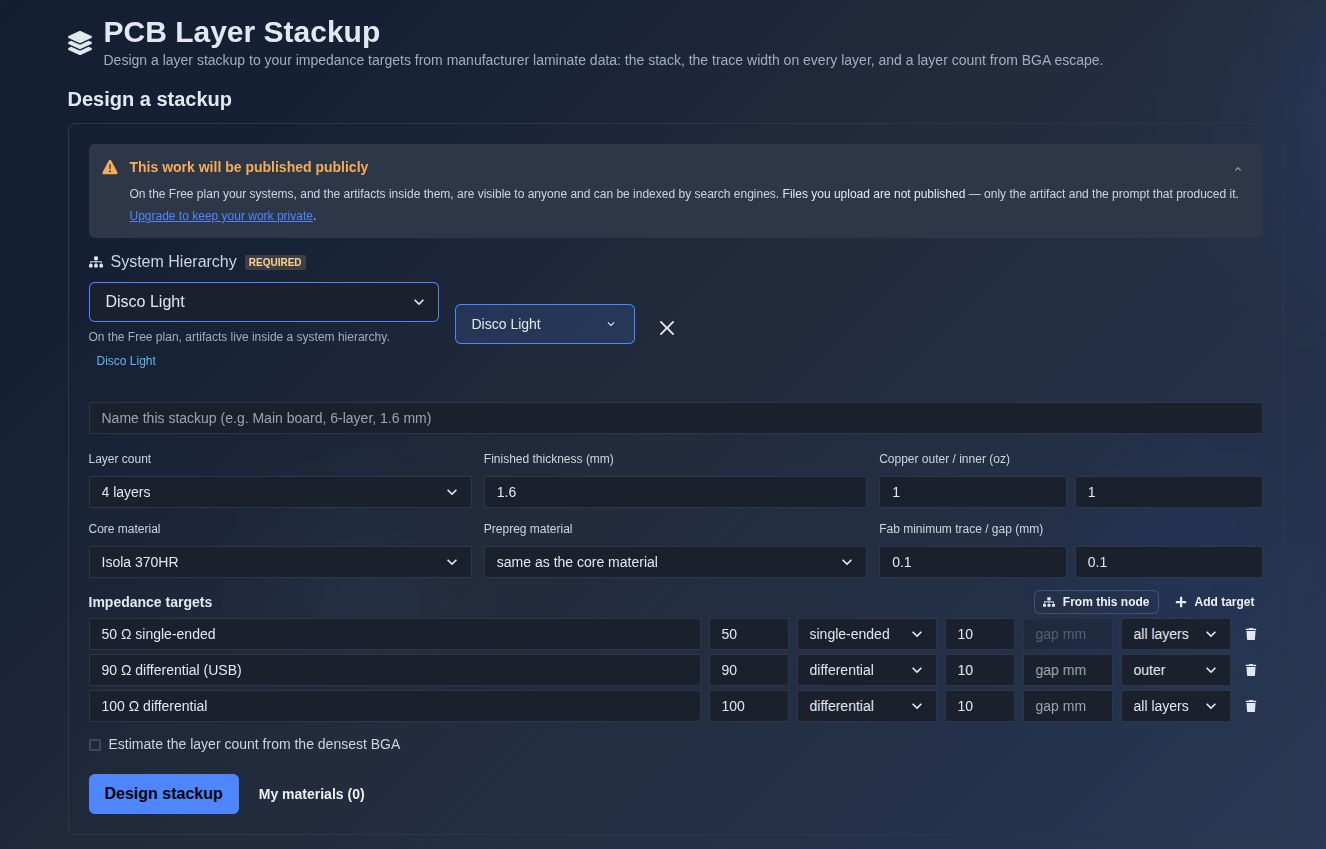
Select a system node and name the stackup. → Optionally select a system and node from the “System Hierarchy” so the stackup belongs to that node. Enter a name for the stackup, for example “Main board, 6-layer, 1.6 mm.” Previously designed stackups are listed under “Past stackups,” where they can be opened, renamed, or deleted.
▶ Select a system node and name the stackup▼ Select a system node and name the stackup
-
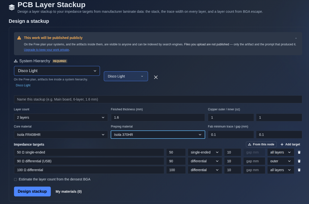
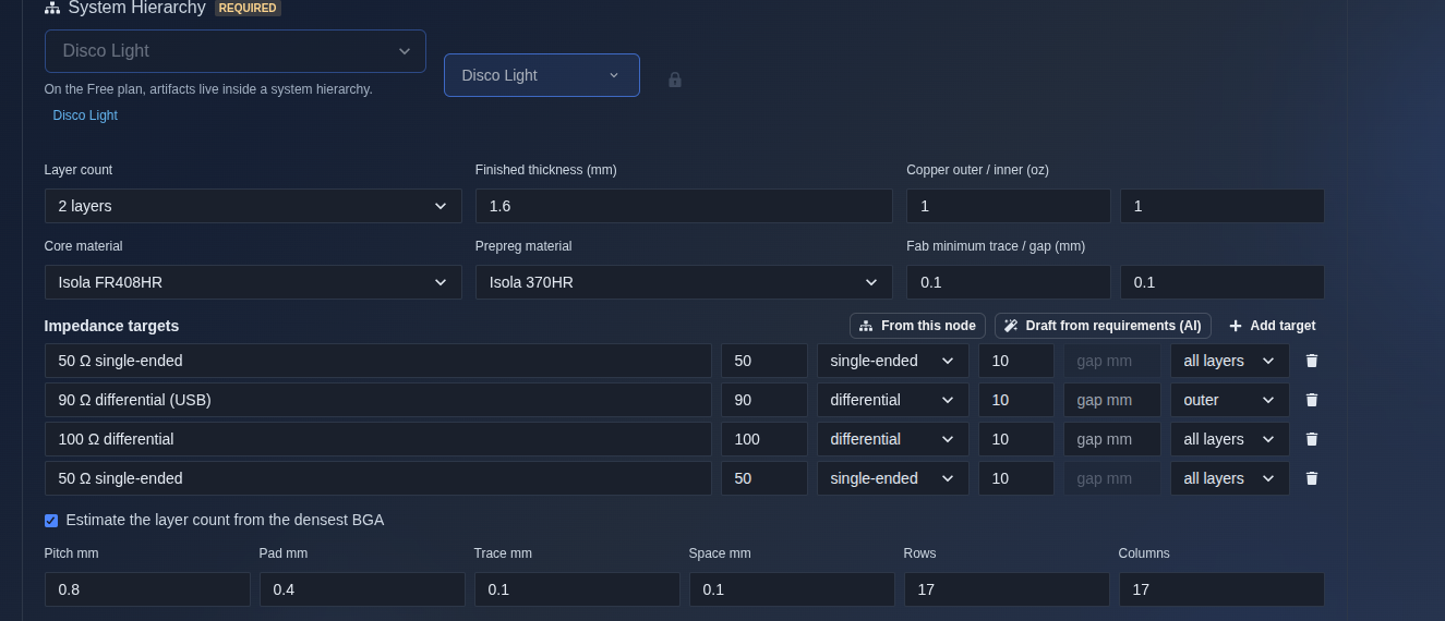
Set the board inputs. → Choose the “Layer count” (2, 4, 6, 8, 10, or 12 layers, or “Recommend from BGA escape”), the “Finished thickness (mm),” the outer and inner copper weight (oz), the “Core material” and “Prepreg material” from the manufacturer laminate catalog, and the fabricator’s minimum trace width and gap (mm). Prepreg defaults to the same family as the core; a core-only laminate requires a prepreg to be chosen.
▶ Set the board inputs▼ Set the board inputs
-
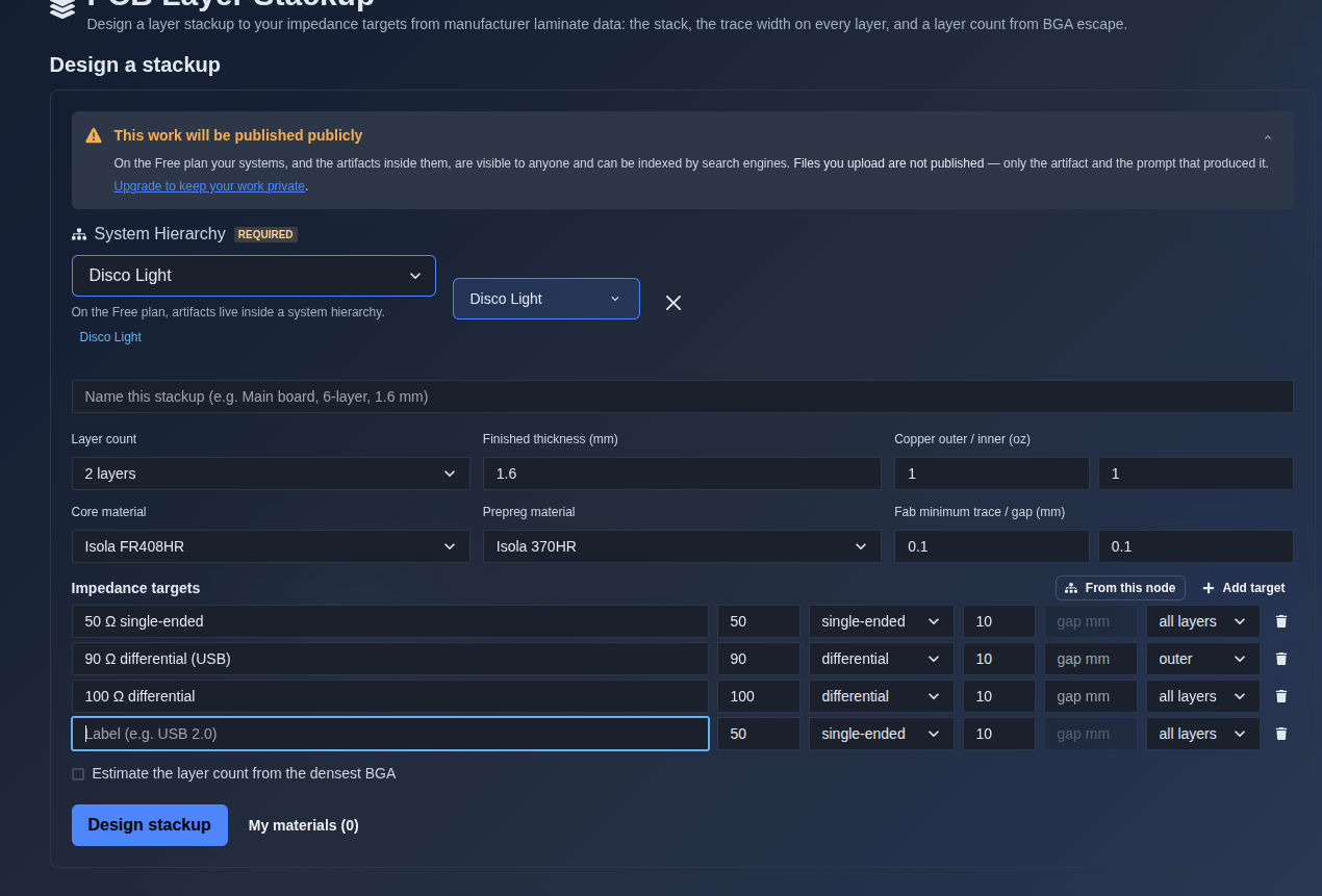
Add the impedance targets. → Under “Impedance targets,” the defaults are 50 Ω single-ended, 90 Ω differential (USB), and 100 Ω differential. Click “Add target” to add up to 20 targets, each with a label, ohms, single-ended or differential mode, ± tolerance %, a gap for differential pairs, and the layers it applies to (all, outer, or inner). Click “From this node” to import the impedances already stated on the node’s Implementation Workspaces (declared in Net assumptions or from an impedance net class).
▶ Add the impedance targets▼ Add the impedance targets
-
Optionally estimate the layer count from a BGA. → Tick “Estimate the layer count from the densest BGA” and enter its pitch, pad, trace, space, rows, and columns (mm). The tool shows the escape-routing arithmetic under “Layer count from BGA escape (estimate)” and uses the result when the layer count is set to “Recommend from BGA escape.”
▶ Estimate the layer count from a BGA▼ Estimate the layer count from a BGA
-
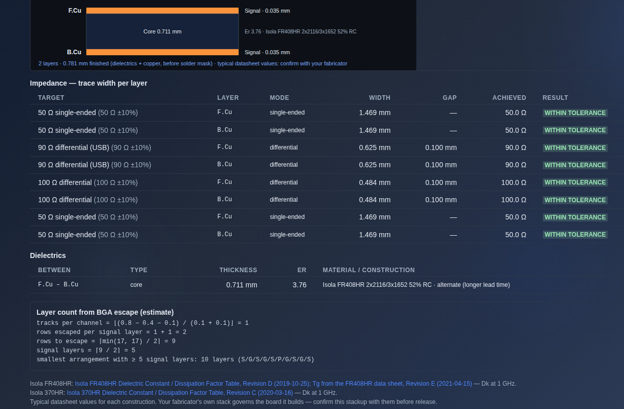
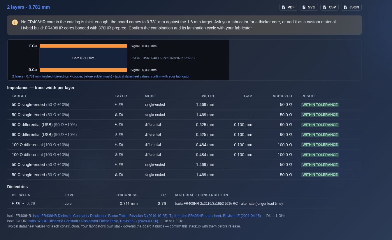
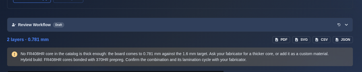
Click “Design stackup.” → The stackup is computed from the laminate data and shown as a stackup drawing (copper layers with their roles, cores, and prepregs with thickness and Dk) and the finished thickness. The “Impedance — trace width per layer” table gives, for each target and layer, the width, gap, achieved impedance, and a result of within tolerance, out of tolerance, or infeasible (with the reason). The “Dielectrics” table lists each dielectric with the layers it sits between, its type, thickness, Er, and material / construction. Any problems or warnings are shown above the results.
▶ Click “Design stackup”▼ Click “Design stackup”
-
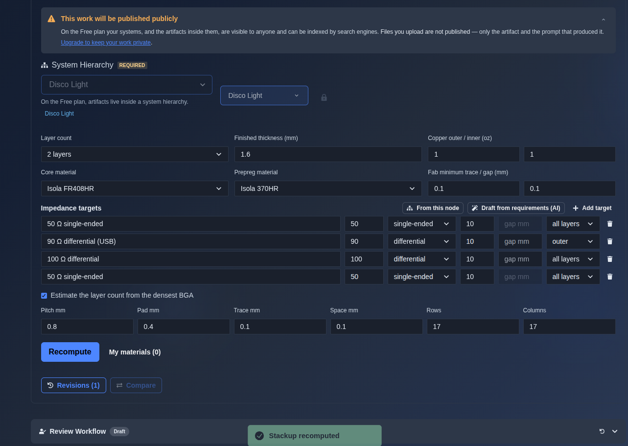
Change inputs and recompute. → Edit the inputs and click “Recompute” to re-run the design. If the stackup is baselined, the new design is staged as a working copy; review it, then click “Merge into stackup” or discard it. Revisions can be viewed as read-only snapshots and restored.
▶ Change inputs and recompute▼ Change inputs and recompute
-
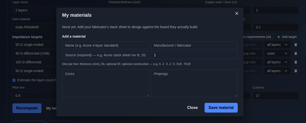
Add your fabricator’s materials. → Click “My materials” and “Add a material” to enter your fabricator’s stack sheet: name, manufacturer, source (required), Dk frequency (GHz), and one line per core and prepreg with thickness (mm), Dk, optional Df, and optional construction (for example “0.2 4.2 0.018 7628”). Saved materials appear in the core and prepreg selectors marked “(mine).”
▶ Add your fabricator’s materials▼ Add your fabricator’s materials
-
Export the stackup. → Click “PDF” for a formatted document with the stackup drawing, “SVG” for the drawing alone, “CSV” for the impedance table, or “JSON” for the full structured data.
▶ Export the stackup▼ Export the stackup
Mechanics
- Layer count 2–12, or recommended from BGA escape routing
- Manufacturer laminate catalog (core + prepreg), plus your own fabricator materials
- Up to 20 impedance targets · single-ended / differential · ± tolerance · all / outer / inner layers
- Import stated impedances from the node’s Implementation Workspaces
- AI-drafted targets from the node’s requirements and ICD, each citing its source
- Stackup drawing · impedance table (width, gap, achieved Ω, within / out of tolerance / infeasible) · dielectrics table
- Recompute · working copy & merge on baselined stackups · revisions & restore
- Review workflow
- Export: PDF · SVG · CSV · JSON